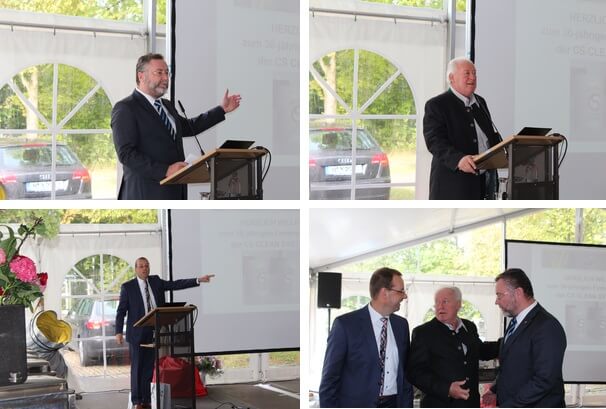
On Friday the 14th of October CS CLEAN SYSTEM AG celebrated their 30 anniversary and the inauguration of an additional building for the re-fill department. Most international sales partners who had their annual group meeting the day before also took part in the celebration.
As representative of the municipality, Mayor Dr. Alexander Greulich addressed the good relations between the community and CS CLEAN SYSTEMS AG. The next speaker, company founder Dr. Christoph Scholz, had many interesting thing to say about the company’s history.
The CEO of CS CLEAN SYSTEMS AG, Georg Lipperer, finally added an overview of recent activities, the status quo and future prospects. After that, of course, there was a buffet and drinks. As well as some live music as background for many interesting conversations.
At the end of the party, every guest received a CS beer mug as a souvenir.
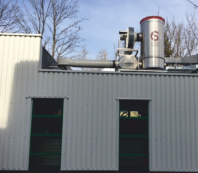
CS CLEAN SOLUTIONS AG recently announced the opening of a new facility for the refurbishment and service of waste gas treatment columns. Opening of the modernized facility at its Ismaning (Munich) headquarters follows successful completion of a 12-month trial phase.
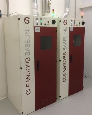
Unused process gases and hazardous by-products from plasma etch, CVD and similar semiconductor processes must be removed efficiently and safely from exhaust lines to ensure safety of personnel and compliance with regulatory emission standards. For over 30 years, users of the CLEANSORB® range of dry scrubber products in Germany, Austria and Switzerland have enjoyed a comprehensive maintenance package comprising a unique take-back and disposal service for the spent absorber material. Similar customer support is available in other countries through the CS CLEAN SOLUTIONS network of local service centres.
Expansion of the service centre at the Munich facility was necessary to increase throughput and keep pace with the steady growth in semiconductor research and processing in recent years, particularly in the III-V sector. The modernized facility has been re-built from scratch in a dedicated building which is equipped to the highest standards of operator safety and materials handling. The CLEANSORB® waste gas abatement system removes hazardous process gases by chemical conversion to stable solids at ambient temperature (chemisorption). No external heating, waste water, or other facilities are required for operation. Hence, the CLEANSORB® system is fully passive, and is permanently on standby, even in the event of a power- or other facilities failure.
CS CLEAN SOLUTIONS AG Ismaning (Munich) headquarters
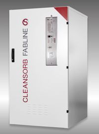
CS200FS FABLINE for the purification of exhaust gases
The CLEANSORB® exhaust gas abatement systems CS200FS FABLINE for the purification of exhaust gases from different PECVD processes were installed in 2015 and 2016. The institute is the transfer point for research, development and service to production scale and is therefore strongly involved in technology transfer to the industry. In addition to efficiency, operator guidance and communication with the process equipment, it is decisive that the exhaust gas abatement systems are not only suitable for research applications but also for industrial scale production. Like other high-tech semiconductor production the manufacturing of silicon solar cells involves the use of special process gases, the majority of which are pyrophoric, toxic, or corrosive. Thus, personnel safety and protection of the environment are matters of the highest priority. Therefore, the exhaust gas abatement system CLEANSORB® CS200FS FABLINE by CS CLEAN SOLUTIONS AG, who have more than 30 years of experience in the semiconductor industry, was installed in the new PV Lab. The CLEANSORB® waste gas abatement system removes hazardous process gases by chemical conversion to stable salts at ambient temperature (chemisorption). No external heating, moisturization, or other facilities are required for operation. Hence, the CLEANSORB® system is fully passive, and is permanently ready to abate, even in the event of a power- or other facilities failure. In addition, the maintenance is done by CS CLEAN SOLUTIONS personnel and the refilling of consumed CLEANSORB® modules in their local Refill Service Center.
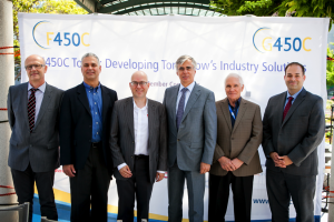
Last Tuesday at SEMICON West, the Facilities 450mm Consortium hosted a panel of representatives from F450C and G450C member companies to provide an update on fab facilities and infrastructure progress in preparing for the transition from 300mm substrates to 450mm. As the F450C Program Manager, I was honored to moderate the panel which included David Skilbred, Director of Program Coordination/Management, G450C (Intel assignee); Ben Peek, F450C Project Architect from Haws; Lothar Till, Managing Director for Ovivo Switzerland; Paul Alers, Head of Product Management for Busch Vacuum; and Joe Guerin, Head of Sales and Marketing for CS CLEAN SYSTEMS (read more).
from left: Joe Guerin, Head of Sales and Marketing for CS CLEAN SYSTEMS; Todd Fosler, F450C Program Manager; Paul Alers, Head of Product Management for Busch Vacuum; Lothar Till, Managing Director for Ovivo Switzerland; Ben Peek, F450C Project Architect from Haws; and David Skilbred, Director of Program Coordination/Management, G450C (Intel assignee)
AB Mandal are pleased to announce the opening of their new CS CLEAN SYSTEMS change facility in Sydney. The new facility supports existing CS CLEAN SYSTEMS abatement equipment customers and enhances the viability of their abatement offerings in Australia. It includes a purpose built change out booth with the capability to safely change out spent granulates and service columns. The booth was designed in close consultation with CS CLEAN SYSTEMS technical support staff in Germany who also provided training for AB Mandal staff.
AB Mandal will stock bulk granulates and spare components for filling CLEANSORB columns and CLEANVENT cartridges to ensure a quick turn around and economical change out.
Australian CS CLEAN SYSTEMS customers will now have the peace of mind knowing that their columns can be changed out quickly and that spent granulate will be safely disposed of or recycled according to local regulations.
In transitioning from 300mm to 450mm wafer processing, the surface area of each wafer approximately doubles and so the mass of direct materials used in deposition and etch chambers can be expected to increase accordingly. Consequently, the cost to deliver and abate process chemicals will likewise double…unless we re-examine how our process tools are integrated into our fab facilities. The abatement of toxic effluent gases from deposition and etch chambers is an ongoing challenge for fabs, and there are different “optimal” solutions depending on whether we take a unit-process or a total-fab perspective… read more
In 2014 the exhaust gas abatement system CLEANSORB® from CS CLEAN SYSTEMS was installed at the Russian MAPPER MEMS production plant for electron beam lithography.
MAPPER Lithography, founded out of Delft University of Technology, is a Delft-based company focusing on the introduction of a groundbreaking maskless lithography infrastructure for the semiconductor industry. Its tools utilize an innovative multiple e-beam technology with which next generation semiconductors can be manufactured more cost effectively. Whereas traditional optical lithography technology requires the use of a costly mask (up to €2 million per chip module), MAPPER’s machines eliminate its necessity. Especially end-users of chips made in relatively low volumes, such as chips for mobile phones and cars, benefit from a maskless solution, since the mask costs are dominating the total costs. The e-beam technology combines high resolution and high productivity – up to 100 wafers per hour – with a lower cost in production.
In 2012 Russian Corporation RUSNANO along with other funds invested in the company MAPPER Lithography. RUSNANO’s investment part was used to establish a manufacturing site in Russia for MAPPER’s lens components. The micro electromechanical (MEMS)-based lens components system, one of MAPPER’s major innovations, can ultimately operate with more than 13,260 parallel electron beams simultaneously. The Russian MEMS fab is opened in a new Russian high technology center Technopolis Moscow, located on the territory of the former car factory in close proximity from the Moscow city center.
MEMS elements manufacturing, as well as any other high-tech semiconductor production, involves the use of special process gases, whereas the majority of them are pyrophoric, toxic, or corrosive. Thus, safety of personnel and protection of the environment are matters of the highest priority. Therefore, the exhaust gas abatement system CLEANSORB® from CS CLEAN SYSTEMS, which has more than 25 years of experience in semiconductor industry, was installed at the new MEMS plant.
The CLEANSORB® waste gas abatement system removes hazardous process gases on the basis of chemical conversion (chemisorption) to stable salts at ambient temperature. No external heating, moisturisation, or other facilities are required for operation. Hence, the CLEANSORB® system is fully passive, and is permanently on stand-by, even in the event of a power- or other facilities failure. In addition, an important factor in choosing this particular system was the fact that the maintenance and refilling of used-up modules CLEANSORB is carried out in Moscow by Russian authorized personnel from Sigm Plus Co.
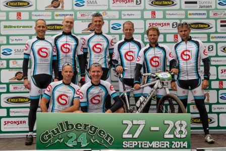
This year again, our Dutch partners took part in the 6 hours race in Gulbergen in the Netherlands. And they even topped last year’s performance: they became number One in the sportteam and funteam categories!
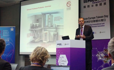
This year’s Silicon Europe Taiwan Day was organised by the EU Business and Regulatory Cooperation Programme in Taiwan (EBRC). This half-day event brought together key industrial and institutional micro- and nanoelectronics players from Europe and Taiwan. Funded by the European Union the EBRC programme concentrates on paving the way for sustainable engagement and cooperation between Europe and Taiwan.
As an invited speaker, Mr. Georg Lipperer (CEO, CS CLEAN SYSTEMS AG) presented the Silicon Saxony organisation as Europe’s most successful trade association for the micro- and nanoelectronics industries. As an SME member in this network he stressed the advantages this platform provides and described CS CLEAN SYSTEMS’ environmentally friendly exhaust gas treatment technology.
Over the past few decades, discrete transistors based on nonsilicon material regimes such as gallium arsenide and indium phosphide have continuously left their silicon counterparts lagging behind in terms of achievable operating frequency. These devices and the diverse industries that fabricate them are known collectively as compound semiconductors (aka III-V devices). While fabricators of such devices had never been shy in proclaiming III-V as “the technology of the future,” manufacturers of silicon-based devices occasionally take joy in adding: “and it always will be.” It seems that as soon as III-V devices begin to capture market share, the silicon industry always finds a way of tweaking that extra-needed speed out of CMOS… read more
Cookie notice
Overview of all cookies used: You can give your consent to entire categories or display further information and select only certain cookies.
Information on data protection and legal notice can be found here. The cookie policy can be found here:
Diese Website verwendet Cookies, um Nutzungskomfort zu verbessern. Von diesen Cookies werden die akzeptierten Cookies im Browser gespeichert, da sie für das Funktionieren der Website unerlässlich sind. Wir verwenden auch Cookies von Drittanbietern, mit denen wir analysieren und nachvollziehen können, wie Sie diese Website nutzen. Diese Cookies werden nur mit Ihrer Zustimmung in Ihrem Browser gespeichert. Sie haben auch die Möglichkeit, diese Cookies zu deaktivieren. Das Deaktivieren einiger dieser Cookies kann sich jedoch auf Ihr Surferlebnis auswirken.
Necessary cookies are essential for the smooth functioning of the website. This category contains only cookies that provide basic functionality and security features of the site. These cookies do not store personal information.
All cookies that are not strictly necessary to the functioning of the website and that are specifically used to collect personal user information through analytics, advertisements, and other embedded content are called non-essential cookies. It is mandatory to obtain the user's consent before using these cookies on your website.
You must be logged in to post a comment.