Atomic Layer Deposition (ALD)
Atomic Layer Deposition (ALD) allows the growth of epitaxial and CVD films to be controlled at the atomic level. The film-forming species are introduced alternatingly into the growth chamber to form monolayers, enabling device structures to be grown at dimensions of 20nm and below.
Deposition of latest generation transistor gates and other critical structures require metal complexes and other large molecules which are only available as liquid organometallic sources. CLEANSORB dry bed chemisorber technology offers a safe, efficient solution for a wide range of gaseous and liquid ALD precursors.
Deposition of latest generation transistor gates and other critical structures require metal complexes and other large molecules which are only available as liquid organometallic sources. CLEANSORB dry bed chemisorber technology offers a safe, efficient solution for a wide range of gaseous and liquid ALD precursors.
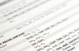
| ALD Process | Typical Gases Used |
|---|---|
| Gate Electrodes | MPA, Ru(Cp)2, PEMAT |
| Low-k Dielectrics | 1MS, 2MS, 3MS, DMDMOS |
| High-k Dielectrics | TMA, TEMAH, TDEAH, TAETO, PET |
| Barrier Layers | TiCl4, NH3, TDMAT, PDMATa, PDEATa, TAETO, W(CO)6 |
