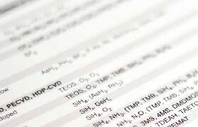
Chemical Vapor Deposition (CVD) is an application used in semiconductor manufacturing to deposit a thin film on the surface of a wafer by means of gaseous compounds. The three forms are PECVD (Plasma-Enhanded CVD), LPCVD (Low-Pressure CVD) and APCVD (Atmospheric-Pressure CVD). Common thin films are poly silicon as semiconductor layer, oxide and nitride als dielectrical layer and metals as conductive layer. In order to grow the dielectrical layers gases like silane, TEOS, oxygen, nitrogen, nitrous oxide and ammonia are used, whereas conductive layers are usually grown with tungsten hexafluoride.
| CVD Process |
Typical Gases Used |
| Oxide / Nitride / Nitrous Oxide |
TEOS, SiH4, NH3, N2O, O2 |
| Tungsten |
WF6, SiH4, H2 |
| Chamber Clean |
NF3, CF4, C3F8, SF6 |